Purpose
The RT2613A is a synchronous step-down converter with the input voltage range from 2.95V to 6V and provides 3A output current. This document explains the function and use of the RT2613A evaluation board (EVB), and provides information to enable operation, modification of the evaluation board and circuit to suit individual requirements.
Introduction
General Product Information
The RT2613A is a high efficiency step-down converter and capable of delivering 3A output current over a wide input voltage range from 2.95V to 6V. The RT2613A provides accurate regulation for a variety of loads with ±3% accuracy. For reducing inductor size, it provides up to 2MHz switching frequency. The efficiency is maximized through the integrated 45mΩ MOSFETs and 550μA typical supply current. Under voltage lockout voltage of the RT2613A is 2.7V, and it also provides external setting by a resistor network on the enable pin. The RT2613A provides protections such as inductor current limit under voltage lockout and thermal shutdown. The over temperature threshold is 145°C. The RT2613A is available in WQFN-16L 3x3 package.
Product Feature
-
Integrated 45mΩ MOSFETs
-
Input Range : 2.95V to 6V
-
Adjustable PWM Frequency : 700kHz to 2MHz
-
Output Current : 3A
-
95% Efficiency
-
Adjustable Soft-Start
-
Power Good Indicator
-
Enable Control
-
Under Voltage Lockout
-
Current Limit
-
Thermal Shutdown
Key Performance Summary Table
|
Key Features
|
Evaluation Board Number : PCB038_V1
|
|
Input Voltage Range
|
2.95V to 6V
|
|
Max Output Current
|
3A
|
|
Default Output Voltage
|
1.8V
|
|
Default Marking & Package Type
|
RT2613AGQW, WQFN-16L 3x3
|
|
Operation Frequency
|
Adjustable from 700kHz to 2MHz
|
Bench Test Setup Conditions
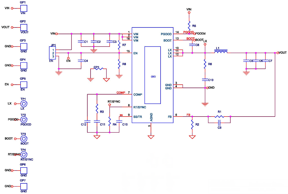
Headers Description and Placement
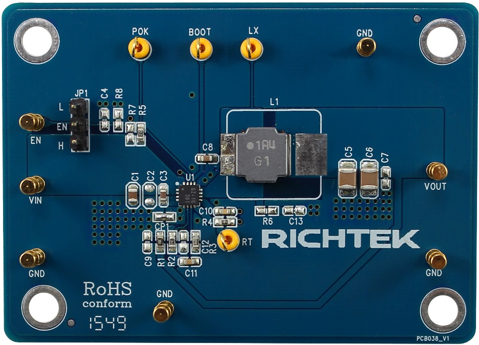
Please carefully inspect the EVB IC and external components, comparing them to the following Bill of Materials, to ensure that all components are installed and undamaged. If any components are missing or damaged during transportation, please contact the distributor or send e-mail to evb_service@richtek.com
Test Points
The EVB is provided with the test points and pin names listed in the table below.
|
Test point/
Pin name
|
Signal
|
Comment (expected waveforms or voltage levels on test points)
|
|
VIN
|
Input voltage
|
Power input.
|
|
EN
|
Enable test point
|
Externally pulled high to enable and pulled low to disable this chip. It is internally pulled up to high when the pin is floating.
|
|
GND
|
Ground
|
The exposed pad must be soldered to a large PCB and connected to GND for maximum power dissipation.
|
|
AGND
|
Analog ground
|
Analog ground.
|
|
COMP
|
Compensation node test point
|
Compensation node for converter stability.
|
|
FB
|
Feedback voltage input
|
Feedback input.
|
|
PGOOD
|
Power good test point
|
Output of power good indicator.
|
|
BOOT
|
Bootstrap supply test point
|
Bootstrap supply for high-side gate driver. Connect a capacitor between the BOOT and LX pins.
|
|
LX
|
Switch node test point
|
Connect this pin to an external L-C filter.
|
|
RT/SYNC
|
Clock input
|
Frequency Setting and External Synchronous.
|
Power-up & Measurement Procedure
1. Apply a 12V nominal input power supply (2.95V < VIN < 6V) to the VIN and GND terminals.
2. Set the jumper at JP1 to connect terminals 1 and 2, connecting EN to enable operation.
3. Verify the output voltage (approximately 1.8V) between VOUT and GND.
4. Connect an external load up to 3A to the VOUT and GND terminals and verify the output voltage and current.
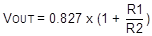
Output Voltage Setting
Set the output voltage with the resistive divider (R1, R2) between VOUT and GND with the midpoint connected to FB. The output is set by the following formula :
Schematic, Bill of Materials & Board Layout
EVB Schematic Diagram
Bill of Materials
|
Reference
|
Qty
|
Part Number
|
Description
|
Package
|
Manufacture
|
|
U1
|
1
|
RT2613AGQW
|
DC/DC Converter
|
WQFN-16L 3x3
|
RICHTEK
|
|
C1
|
1
|
C2012X5R1C106KT
|
10µF/16V/X5R
|
C-0805
|
TDK
|
|
C3
|
1
|
C1608X5R1E105KT000E
|
1µF/25V/X5R
|
C-0603
|
TDK
|
|
C5, C6
|
2
|
GRM32ER61C226KE20L
|
22µF/16V/X7R
|
C-1210
|
MURATA
|
|
C8
|
1
|
C1608X7R1H104KT000N
|
0.1µF/50V/X7R
|
C-0603
|
TDK
|
|
C10
|
1
|
0603B103K500
|
10nF/50V/X7R
|
C-0603
|
WALSIN
|
|
C11
|
1
|
0603B332K500
|
3.3nF/50V/X7R
|
R-0603
|
WALSIN
|
|
L1
|
1
|
NR8040T1R4N
|
1.4µH/7A
|
8 x 8 x 4 mm
|
Taiyo Yuden
|
|
R1
|
1
|
|
11.8k
|
R-0603
|
|
|
R2
|
1
|
|
10k
|
R-0603
|
|
|
R3
|
1
|
|
7.68k
|
R-0603
|
|
|
R4
|
1
|
|
180k
|
R-0603
|
|
|
R5
|
1
|
|
100k
|
R-0603
|
|
|
C2, C4, C7, C9, C12, C13, R6, R7, R8
|
9
|
|
NC
|
|
|
|
CP1
|
1
|
|
0
|
|
|
PCB Layout
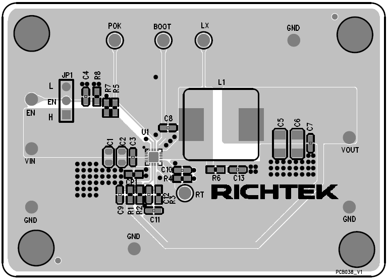
Top View (1st layer)
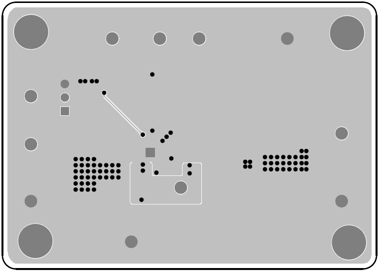
Bottom View (4th Layer)